Devices Fabricated @ IITH
A selection of devices and structures fabricated by students in the NanoX cleanroom, imaged by scanning electron and optical microscopy.
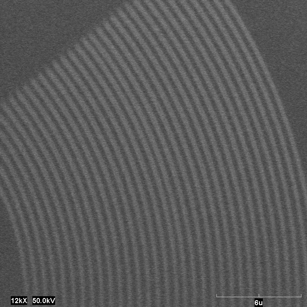
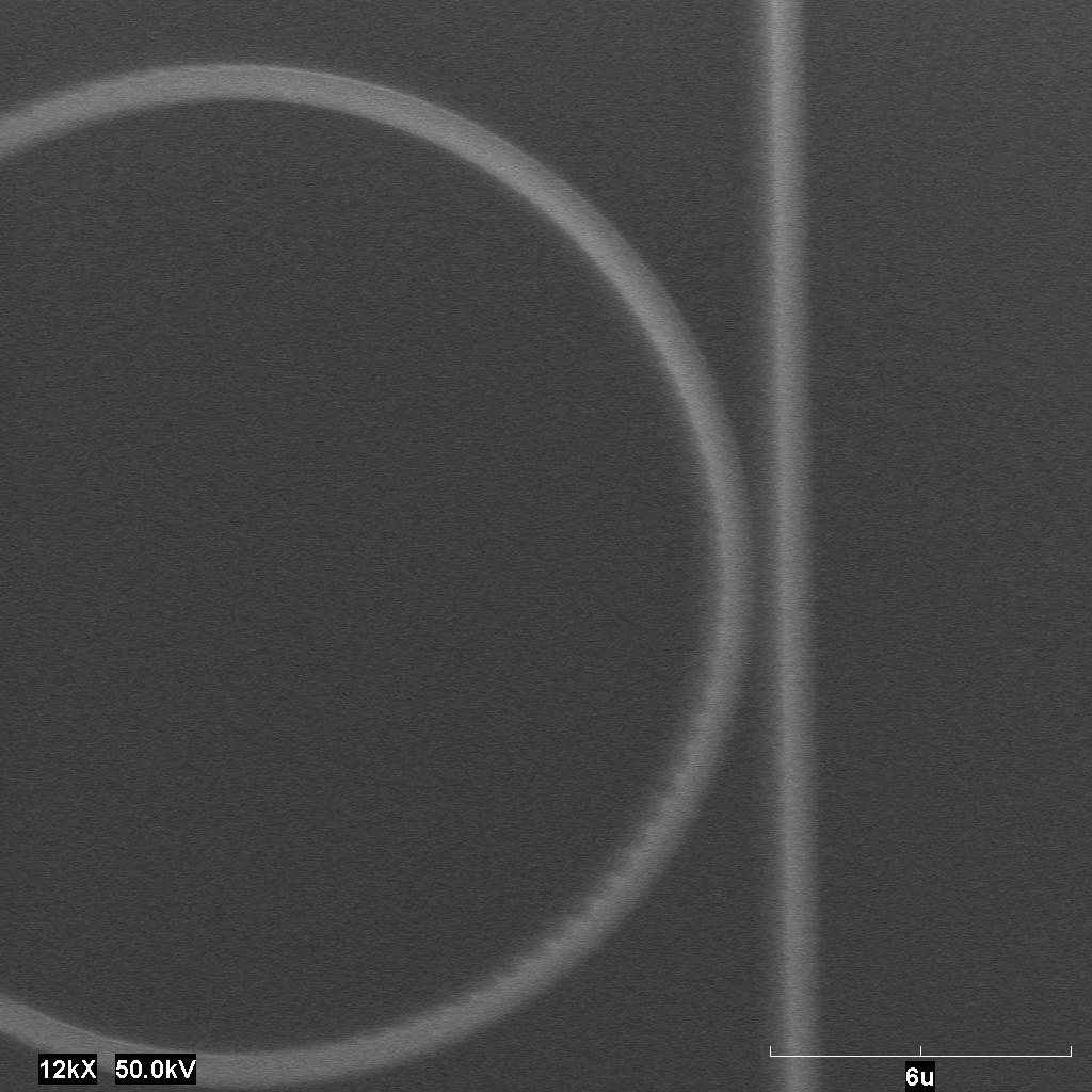
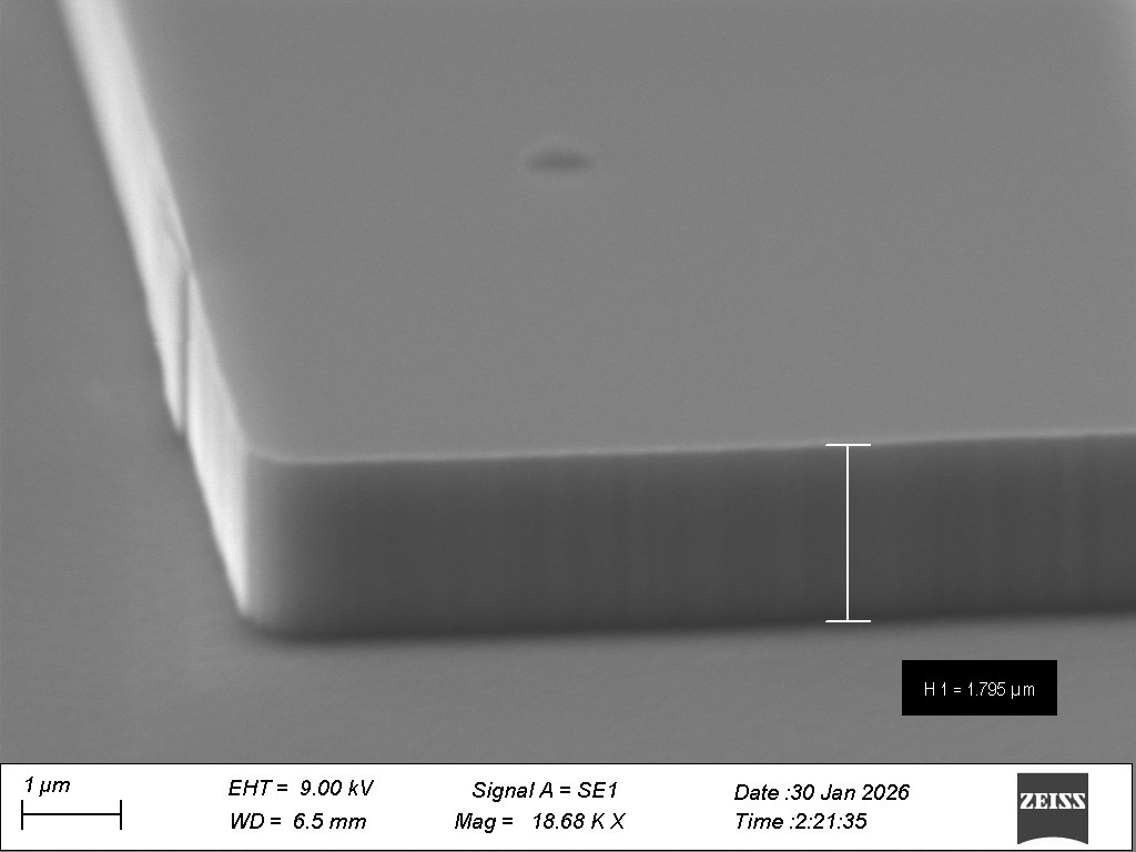
Silicon photonic devices — microring resonator, grating coupler, and dielectric slab waveguide — fabricated for on-chip photonic integrated circuits.
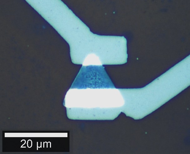
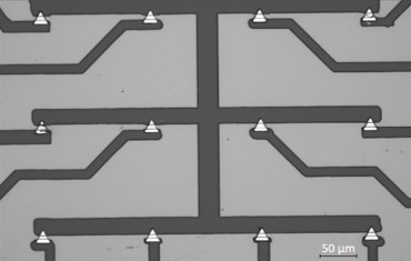
Optical micrographs of transistors fabricated using two-dimensional transition metal dichalcogenide (TMDC) materials.
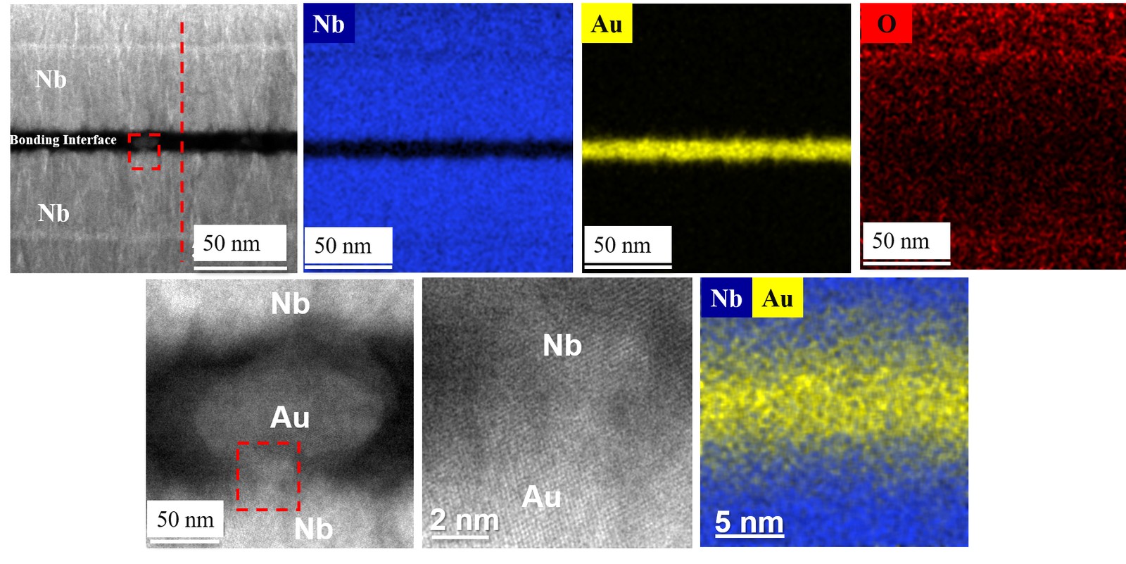
Thermo-compression bonding of Nb–Nb interfaces for 3D quantum processor applications. Cross-sectional TEM imaging and EDS elemental mapping reveal the bonding interface and the distribution of niobium (Nb), gold (Au), and oxygen (O) across it.
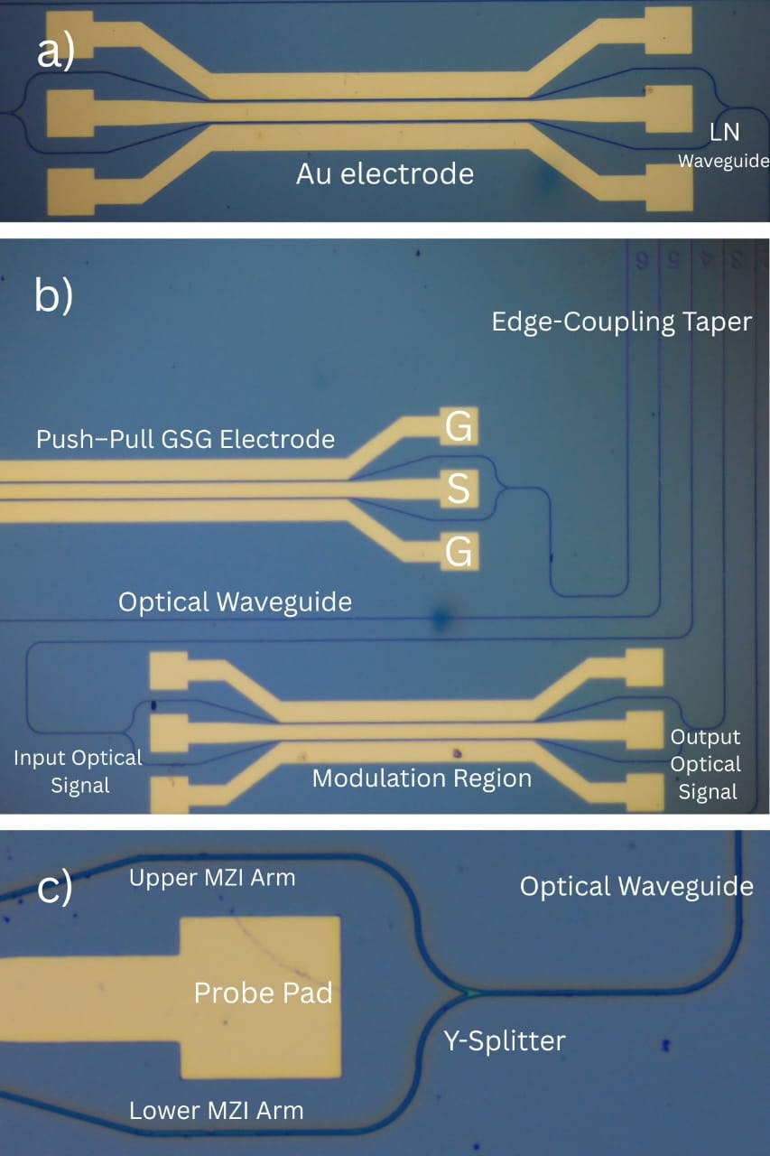
Optical microscope images of the fabricated Lithium Niobate-on-Insulator (LNOI) Mach–Zehnder Modulator (MZM). (a) Gold (Au) electrodes aligned with the 2.5 µm-wide lithium niobate (LN) optical waveguide. (b) MZM showing the edge-coupling taper, push–pull Ground–Signal–Ground (GSG) electrodes, and electro-optic modulation region — the GSG electrodes have a 60 µm signal electrode and 80 µm ground electrodes, with 150×150 µm² probe pads. (c) MZI showing the Y-splitter and upper and lower interferometer arms.
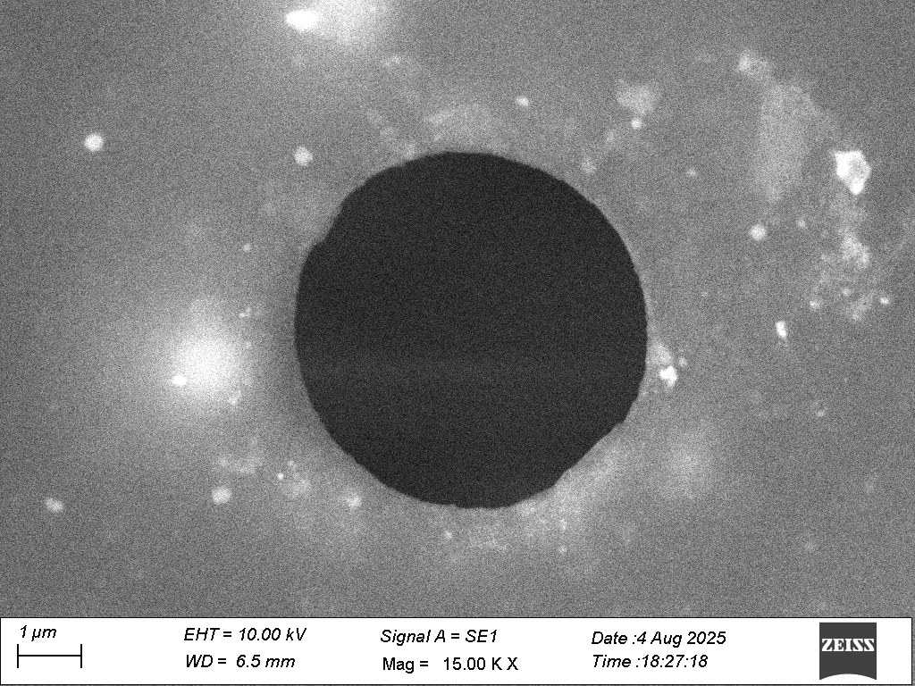
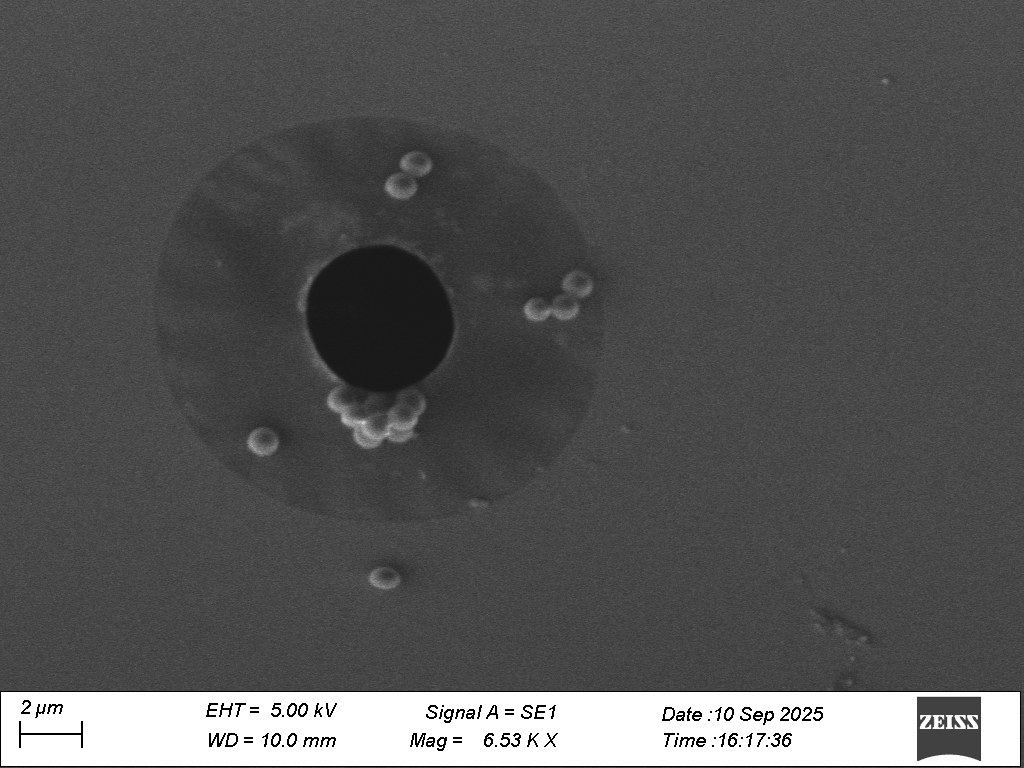
Micropore fabricated in an ultra-thin glass membrane. SEM images confirm the through-hole and show the interaction and accumulation of polystyrene microbeads near the pore, enabling direct visualization of particle transport through the pore for resistive-pulse sensing applications.
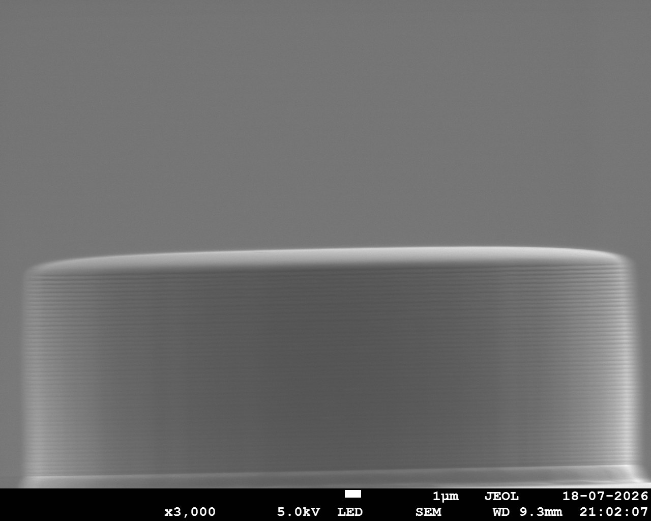
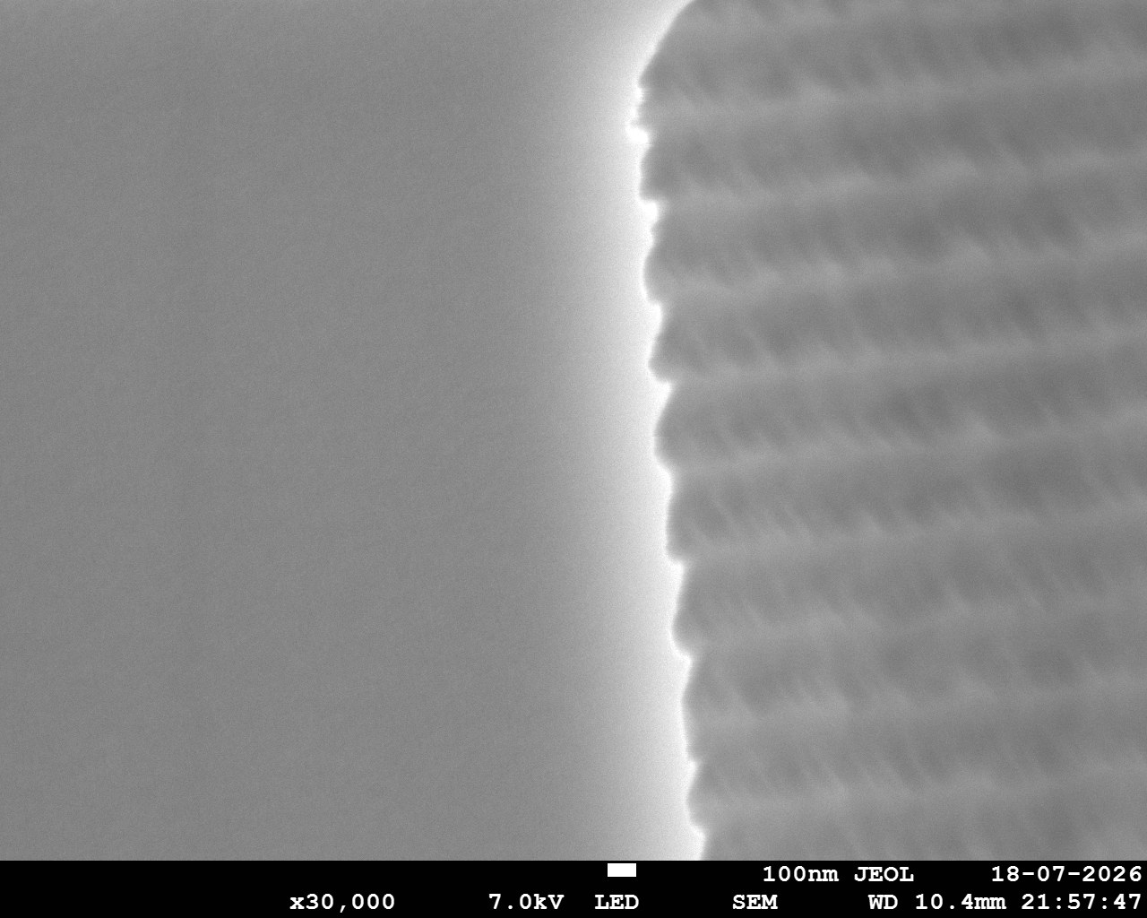
SEM images of silicon deep reactive-ion etching (DRIE); etch depth ~12 µm, pillar diameter ~40 µm. The sidewall scalloping characteristic of the Bosch etch process is visible.
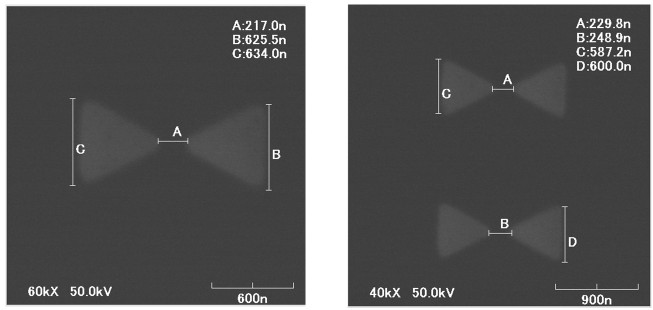
Plasmonic bow-tie antennas fabricated with a gap of ~220 nm using electron-beam lithography.