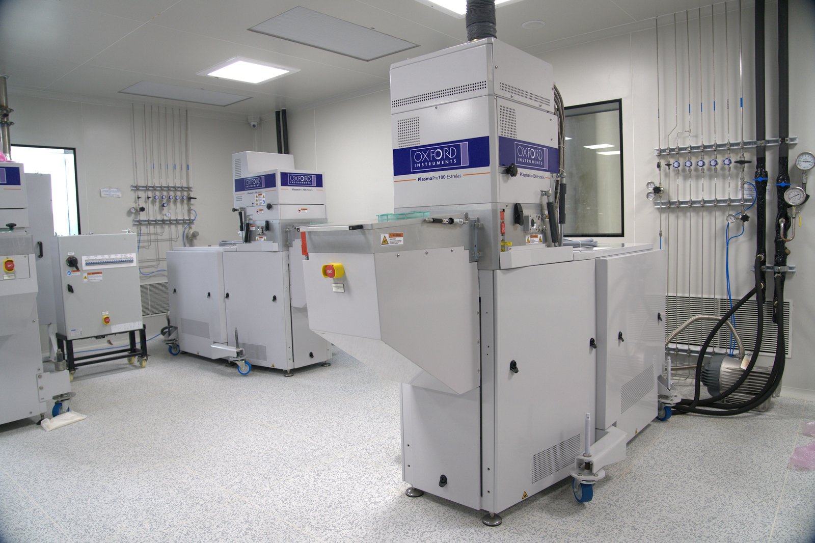
NanoX at IIT Hyderabad is a 2000 sq. ft. fabrication centre housing semiconductor manufacturing tools in a Class 10,000 (approx. 1500 sq. ft.) and a Class 1000 (500 sq. ft.) cleanroom. These tools enable the fabrication of nanoscale devices for research needs — the “X” in NanoX stands for electronic/photonic/MEMS devices. The equipment at the facility is organized into six process technique categories: lithography, deposition, etch, wet processing, 3D integration, and characterisation.
Interested in using the facility? See Using the Facility for how to request access.
Lithography
NanoX offers both optical and electron-beam lithography capabilities for pattern transfer on a range of substrates, forming the foundation of device fabrication in the cleanroom.
Photolithography — SUSS Microtec MA6/BA6 Mask Aligner
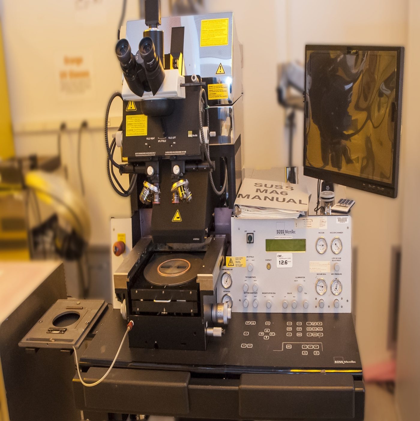
A mask aligner used for contact and proximity photolithography, enabling precise pattern transfer from a photomask onto resist-coated substrates.
Electron-Beam Lithography — CRESTEC CABL-9000C
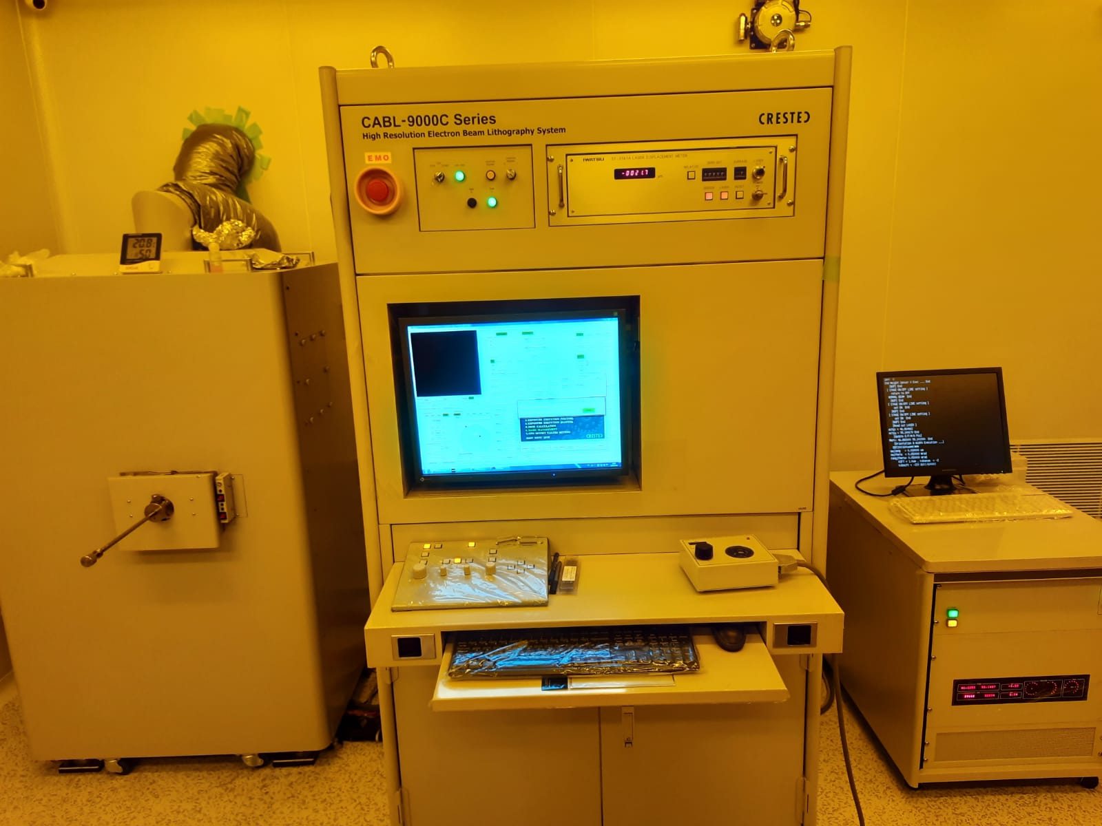
Used to draw custom patterns with sub-10 nm resolution using a focused electron beam.
- Resolution: 2 nm
- Field size: 60 / 120 / 300 / 600 µm
- Minimum line width: 20 nm at 60 µm square field
- Acceleration voltage: 50 kV
- Beam current: 10 pA – 100 nA
- Location: Cleanroom, Annexure C-Block
Deposition
NanoX provides thin-film deposition capabilities used to build up metal and dielectric layers as part of the device fabrication process.
Magnetron Sputtering — AJA International ORION
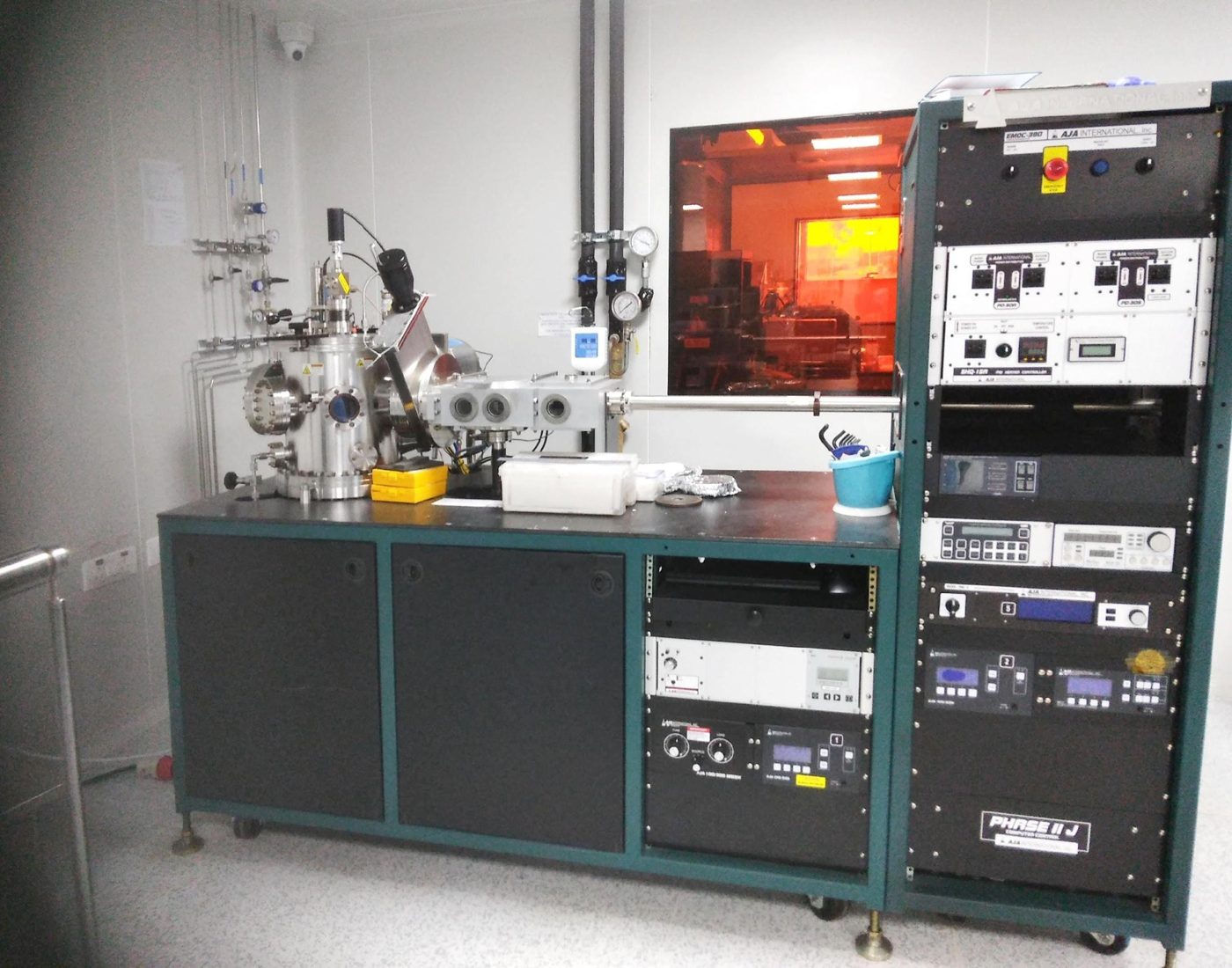
RF and DC magnetron sputtering system for depositing metals and dielectrics.
- Vacuum: Cryo-pumped to 2×10⁻⁸ Torr
- Substrate capacity: 4 inch
- Process gases: Ar, N₂, O₂
- Power: DC magnetron up to 500 W, RF magnetron up to 300 W
- Deposited metals: Gold, copper, titanium, magnesium, chrome
- Deposited dielectrics: Silicon nitride, silicon dioxide
E-Beam Evaporator — VST TFDS-462B
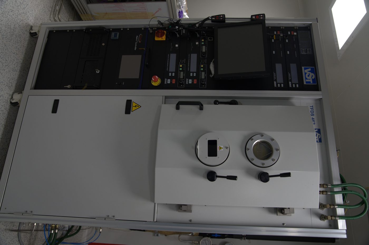
Designed to evaporate metals and dielectrics in a high-vacuum environment (typically 10⁻⁶ Torr), using an electron gun or a thermal source.
- E-gun source: 6 pockets — titanium (Ti), gold (Au), silver (Ag), chrome (Cr), aluminum (Al), SiO₂
- Thermal boat source: Germanium (Ge), gold (Au), copper (typical materials)
- Vacuum system: Roughing pump and cryogenic pump
- Multi-pocket source cooling: Water-cooled (~6 °C)
- Sample holder cooling: Chiller-cooled (~18 °C, can reach lower temperatures)
Etch
NanoX provides etch capabilities to selectively remove material and define device structures as part of the fabrication process.
DRIE Etcher — Plasma Pro 100 Estrelas
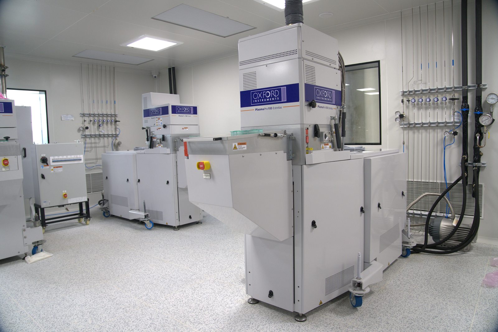
A XeF2-based vapor-phase silicon etcher used for isotropic release etching and deep silicon etching applications.
- Silicon etch rate: 0.1 – 10 µm/min
- Process gas: XeF₂
- Process pressure: 0–6 Torr with XeF₂
- Chamber size: 150 mm diameter
- Etch mask materials: SiO₂, photoresist
- Etch rate (100 mm wafer, 100% open area): 800 Å/cycle
- Selectivity: Si : SiO₂ ≈ 1000 : 1, Si : Si₃N₄ ≈ 100 : 1
- Supports long undercuts (> 100 µm); no stiction associated with the (dry) etch process
Note: this system is not intended for deep silicon etching applications.
Wet Processing
Wet processing equipment at NanoX is being documented and will be listed here soon.
3D Integration
NanoX provides precision wafer bonding capabilities used for MEMS packaging, heterogeneous integration, and device fabrication requiring wafer-to-wafer alignment and bonding.
Wafer Bonder — AML AWB-04
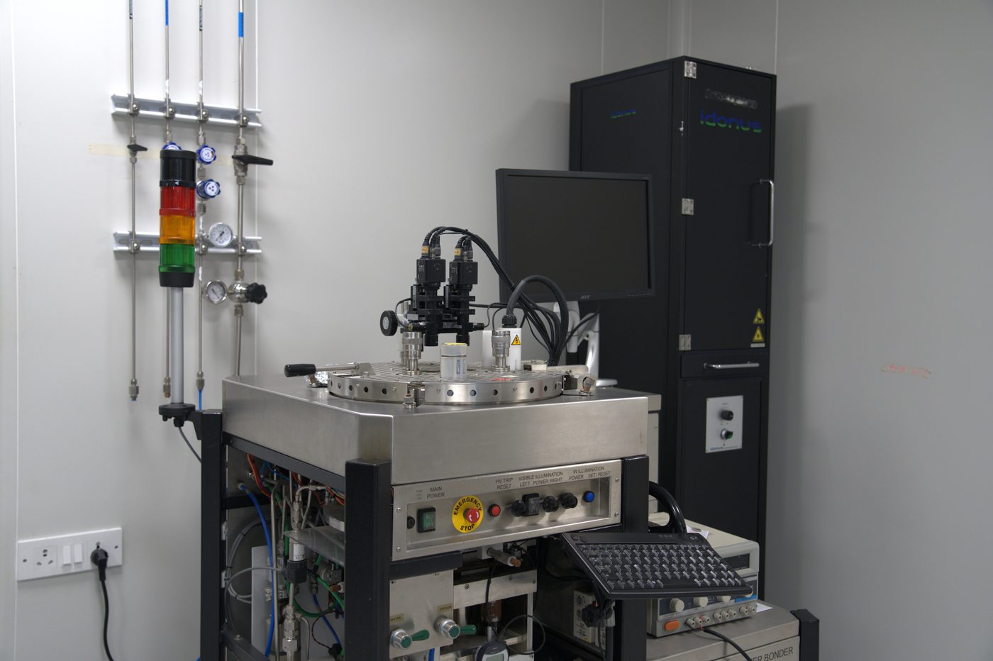
An aligner-wafer bonder platform supporting multiple bonding processes (configuration-dependent).
- Alignment: Unique in-situ alignment system (X, Y, Z & θ), up to 1 µm accuracy
- Control: Automatic PC control & data acquisition
- Voltage: Up to 2.5 kV (anodic bonding)
- Temperature: Up to 560 °C
- Force: Up to 15,000 N
- Vacuum: Self-contained dry pumping system, up to 10⁻⁶ mBar
- Cooling: Forced nitrogen cooling
- Wafer size: 2" to 4"
- Automatic alignment system
Characterisation
Characterisation and metrology equipment at NanoX is being documented and will be listed here soon.
Cleanroom & Facility